
Process & Material
Conductive Silicon Carbide Micro EDM Feasibility Review
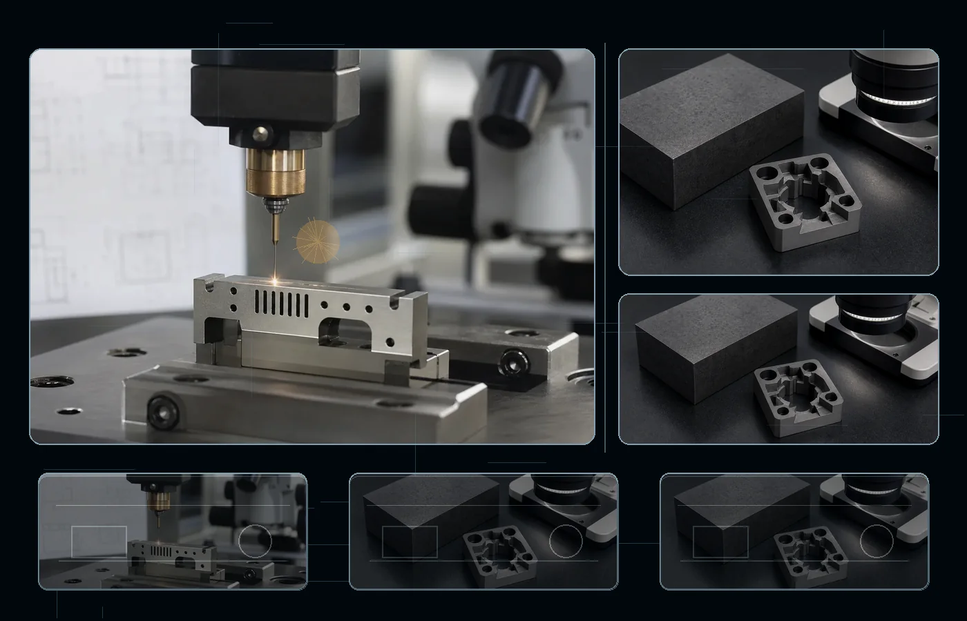
Conductive Silicon Carbide can be machined with Micro EDM when the geometry matches micro holes, micro slots, miniature cavities, fine pins, and sub-millimeter precision details. Conductive Silicon Carbide is an electrically conductive ceramic composite grade that can be EDM processed only when its resistivity supports stable discharge; the supplied condition affects support, discharge energy, finishing, and inspection.
Quick Answer
Micro EDM is suitable for Conductive Silicon Carbide when the feature is a micro hole, micro slot, miniature cavity, fine pin, or other sub-millimeter detail. The supplied condition must be stated before tolerance and surface requirements are confirmed.
Key Material Decisions
How This Material Behaves
An electrically conductive ceramic composite grade that can be EDM processed only when its resistivity supports stable discharge. In Micro EDM, the supplied condition directly changes discharge stability, electrode wear, edge quality, and the finishing plan—especially at micro scale.
Choosing the Right Condition
Choose Micro EDM for micro holes, micro slots, miniature cavities, fine pins, and sub-millimeter precision details. State the exact Conductive Silicon Carbide condition, then set tolerance, finish, support, and inspection from the controlled feature rather than the whole part.
Risks to Manage
For Micro EDM, ceramic brittleness, porosity and edge chipping can dominate even when conductivity is adequate. Temperature drift and electrode calibration can consume the remaining dimensional allowance before the feature is measured as micro-flushing, temperature and metrology become part of the same tolerance chain; acceptance must focus on grain boundaries, brittle rims and subsurface damage zones. On Conductive Silicon Carbide, the resulting defect can be feature discontinuity, pullout or crack damage at a scale comparable with the microstructure. For Conductive Silicon Carbide, use conservative discharge energy, strong local support and microscopic inspection of edges and subsurface damage. Separate true geometry from edge rounding, residue and measurement uncertainty; document geometry, chipping, grain pullout and subsurface cracking for Conductive Silicon Carbide.
How Micro EDM Works on Conductive Silicon Carbide
Micro EDM uses a very small electrode and low discharge energy to machine miniature features in Conductive Silicon Carbide. Electrode wear, spark-gap stability, micro-flushing, temperature control and measurement resolution consume a significant share of the available tolerance. The local feature size and aspect ratio—not the overall workpiece size—must define the route.
Micro EDM Capability Reference
| What you're asking | What you can expect |
|---|---|
| Feature types | micro holes, micro slots, miniature cavities, fine pins, and sub-millimeter precision details |
| Tolerance | ±0.002–0.010 mm |
| Surface finish | Ra 0.1–1.6 μm |
| Feature scale | Sub-millimeter holes, slots, and cavities |
| Primary micro limit | Electrode wear and measurement resolution |
| Main limitation | Loose-tolerance or easily accessible features are rarely economical with Micro EDM. |
Material Condition Reference
| Condition | What to expect | Watch out for | Surface notes |
|---|---|---|---|
| as-sintered or supplied condition | Use low-force fixturing and conservative discharge energy. | Brittle edges can chip or binder-rich zones can erode unevenly. | Inspect edge breakout and surface integrity rather than Ra alone. |
| stress-relieved or recrystallized | Use stable support and reduced energy on finished stock. | Grinding stress or porosity can cause local cracking. | Apply selective polishing or lapping where practical. |
| ground or finished condition | Protect the final surface condition. | Coated, polished, or dense finished surfaces can be damaged by aggressive roughing. | Keep finishing local to the controlled feature. |
How This Material Behaves
Conductive silicon carbide is an electrically machinable ceramic only when its grade provides sufficient conductivity. In EDM, this means brittle fracture and thermal cracking, not hardness, set the practical limit; pores or secondary phases can also create uneven erosion. Confirm the exact conductive grade, support fragile edges, use low-energy finishing, and inspect cracks and grain pullout directly. For Micro EDM, ceramic brittleness, porosity and edge chipping can dominate even when conductivity is adequate. At micro scale, grain size, porosity or binder response can be comparable with the feature itself, making microscopy part of dimensional acceptance.
Surface Integrity and Post-Process
For Micro EDM on Conductive Silicon Carbide, use conservative energy, strong support and inspection focused on edge chipping and subsurface damage. Use low-energy finishing and account for electrode replacement or calibration before final sizing. Specify edge, recast and post-process requirements only on functional microfeatures, and use metrology that can distinguish true size from edge rounding and surface residue.
Conductive Silicon Carbide Micro EDM Checkpoints
- Confirm that the feature matches micro holes, micro slots, miniature cavities, fine pins, and sub-millimeter precision details.
- State the supplied condition: as-sintered or supplied condition, stress-relieved or recrystallized, and ground or finished condition.
- Mark the controlled dimensions, functional surfaces, datum scheme, and inspection method.
Typical Parts and Features
- wear inserts
- high-temperature contacts
- hard-metal nozzles
- micro holes
- micro slots
- miniature cavities
Limits and Better Alternatives
Main Limit
Loose-tolerance or easily accessible features are rarely economical with Micro EDM. On Conductive Silicon Carbide, ceramic brittleness, porosity and edge chipping can dominate even when conductivity is adequate; the supplied condition still controls support, finishing, and surface-integrity review.
Consider Another Route When
Use conventional EDM for larger features, precision laser processing for suitable thin geometry, or mechanical micro-drilling where a tool can reach.
Practical Next Step
Send the Conductive Silicon Carbide drawing with condition, controlled geometry, tolerance, functional surface callouts, quantity, and inspection requirements. If the route is unclear, we will compare Micro EDM with the adjacent EDM or conventional process.
Practical Takeaway
Conductive Silicon Carbide is compatible with Micro EDM when the feature matches the process access. The supplied condition determines support, finishing, surface control, and inspection.
Additional Project Information
Include application, destination and end-use notes together with the material, quantity and drawing requirements.
Project Details for Technical Review
Include application and end-use notes when they affect material, inspection, documentation, or export review.
- Process: Micro EDM
- Material: Conductive Silicon Carbide
- Drawing or part sketch
- Material grade
- Thickness / part size
- Quantity
- Tolerance and critical dimensions
- Surface finish or inspection requirement
STEP/STP, DXF, DWG, PDF, IGS/IGES or ZIP.
Confidential drawing review. NDA support available on request.