
Application Review
Small Hole EDM Drilling for Semiconductor Tooling
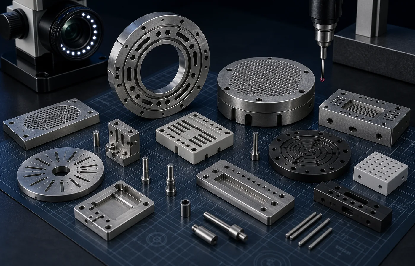
Small Hole EDM is useful in Semiconductor Tooling when the named feature matches small, deep, angled, vent, cooling, or start hole. The decision depends on fine pitch, low particle risk, repeatable alignment and controlled contact or wafer-handling surfaces, the material condition, and the inspection method—not on the application name alone.
Quick Answer
Choose Small Hole EDM for Semiconductor Tooling when the feature is a small, deep, angled, cooling, vent, or start hole in conductive material. Plan the route around flatness, edge condition, micro features, material control, because the main production risk is particle generation, edge damage or pitch accumulation across repeated micro features.
Key Application Decisions
What's at Stake
In Semiconductor Tooling, the feature must support fine pitch, low particle risk, repeatable alignment and controlled contact or wafer-handling surfaces. Small Hole EDM removes the feature without cutting force, but the main service risk remains particle generation, edge damage or pitch accumulation across repeated micro features. The process is justified only when its access and surface behavior solve that specific problem.
How to Get It Right
Use Small Hole EDM for small, deep, angled, vent, cooling, or start hole. On the drawing, state material and condition, the controlled feature, datum, functional surfaces, and flatness, edge condition, micro features, material control. Select the material from the industry priorities below rather than from a generic conductive-material list.
What Can Go Wrong
If the feature can be made more simply by another process, Small Hole EDM adds cost without improving function. If it is selected correctly but electrode diameter, true path depth, aspect ratio, flushing, rotation, straightness, and breakthrough support are not planned, the hole can wander, taper, break out poorly, or carry an unacceptable wall condition when depth, flushing, or support is underestimated. In Semiconductor Tooling, the result may be a rejected datum, damaged functional edge, unstable fit, or failed application-specific inspection.
How EDM Fits the Application
Small Hole EDM rotates a tubular electrode and pumps dielectric through its center, so debris leaves from the advancing tip instead of traveling around a mechanical drill. For Semiconductor Tooling, this solves the difficult-hole part of fine pitch, low particle risk, repeatable alignment and controlled contact or wafer-handling surfaces: hard alloys and long paths can be drilled without drill thrust or a broken tool left in the component. Entry, exit, taper, and wall condition are then inspected to control particle generation, edge damage or pitch accumulation across repeated micro features.
Small Hole EDM Capability Reference
| What you're asking | What you can expect |
|---|---|
| Feature types | small through holes, deep holes, angled holes, cooling holes, vent holes, and start holes in hard or heat-resistant alloys |
| Tolerance | ±0.010–0.050 mm |
| Surface finish | Hole-wall finish is feature-dependent |
| Typical diameter | About 0.3–3.0 mm for ordinary planning |
| Depth driver | Depth-to-diameter ratio, straightness, and breakthrough |
| Main limitation | Very small diameter combined with extreme depth may require specialized equipment, staged electrodes, and dedicated metrology. |
Semiconductor Tooling Application Planning
| What matters | What to expect |
|---|---|
| Typical parts | probe-card tooling, wafer-handling fixtures, lead-frame inserts, and precision alignment plates |
| Functional requirement | fine pitch, low particle risk, repeatable alignment and controlled contact or wafer-handling surfaces |
| Main failure risk | particle generation, edge damage or pitch accumulation across repeated micro features |
| Inspection focus | flatness, edge condition, micro features, material control |
| Planning context | Fine tooling features commonly concentrate tolerance in the ±0.003–0.015 mm range, with optical or CMM verification selected by feature size. |
Application Context
Material choice for Semiconductor Tooling should follow particle control, flatness, thermal stability, vacuum compatibility, and cleanliness, not a generic list of conductive alloys. 316L stainless: use it for vacuum and cleanroom fixtures; electropolish/passivation and cleanliness may be required. 17-4PH / 15-5PH: use it for high-strength precision locating tools; aging condition must be fixed. 6061 / 7075 aluminum: use it for lightweight plates and low-particle fixtures with coating; soft wear surfaces need protection. Invar 36: use it for thermally stable alignment and metrology fixtures; stress relief and machining sequence are critical. The selected grade must also suit the Small Hole EDM access and inspection plan. If the material is undecided, send the drawing and service conditions so the alternatives can be compared before quotation.
Functional Surface and Edge Control
For Small Hole EDM in Semiconductor Tooling, inspect the named functional feature rather than the whole part. Separate geometry from edge or surface acceptance, and focus on flatness, edge condition, micro features, material control. The release route should address particle generation, edge damage or pitch accumulation across repeated micro features.
Semiconductor Tooling Buyer Checkpoints
- Identify which Small Hole EDM feature controls fine pitch, low particle risk, repeatable alignment and controlled contact or wafer-handling surfaces.
- Define the datum and inspection method for flatness, edge condition, micro features, material control.
- State material condition, functional surfaces, quantity, drawing revision, and documentation needs before quotation.
Common Applications
- probe-card tooling
- wafer-handling fixtures
- lead-frame inserts
- precision alignment plates
Limits and Better Alternatives
Main Limit
Small Hole EDM is not the right route when the Semiconductor Tooling feature does not match small through holes, deep holes, angled holes, cooling holes, vent holes, and start holes in hard or heat-resistant alloys.
Consider Another Route When
Use mechanical drilling when the tool can reach economically, laser drilling for suitable thin geometry, or Micro EDM for smaller precision holes.
Practical Next Step
For an EDM review of Semiconductor Tooling, send the drawing, material and condition, the Small Hole EDM feature, tolerance, functional surfaces, quantity, and the inspection or documentation requirements.
Practical Takeaway
For Semiconductor Tooling, use Small Hole EDM only where its access and surface behavior solve the actual feature problem. Release the material, functional surfaces, and flatness, edge condition, micro features, material control together.
Check If This Applies to Your Project
Send application notes and a drawing for a project-specific feasibility check.
- Process: Small Hole EDM
- Application: Semiconductor Tooling
- Drawing or part sketch
- Material grade
- Thickness / part size
- Quantity
- Tolerance and critical dimensions
- Surface finish or inspection requirement
STEP/STP, DXF, DWG, PDF, IGS/IGES or ZIP.
Confidential drawing review. NDA support available on request.